Exploring Strong Interface-Induced Spin–Orbit Interaction in Graphene on BiSe₂O₅
Introduction
In the realm of condensed matter physics, the study of spin–orbit interaction (SOI) in graphene has garnered significant attention due to its potential applications in spintronics. Graphene, a two-dimensional material with exceptional electronic properties, intrinsically exhibits weak SOI. However, when interfaced with other materials, its SOI can be enhanced. This blog post delves into my ongoing research project at Xi’an Jiaotong University (XJTU), focusing on inducing strong interface-induced SOI in graphene by stacking it on bismuth selenium oxide (BiSe₂O₅).
Graphene’s unique electronic structure makes it an excellent candidate for investigating SOI phenomena. Previous studies, such as those involving graphene on transition metal dichalcogenides (TMDs) like WS₂ and WSe₂, have demonstrated an enhancement of SOI due to proximity effects. Inspired by Professor Zhe Wang’s work on these materials, our research aims to explore a similar enhancement by interfacing graphene with BiSe₂O₅, a material known for its strong spin–orbit coupling.
Device Fabrication
To study the interface-induced SOI, we designed a device structure where monolayer graphene is stacked on top of BiSe₂O₅. The schematic of the device structure is presented below:
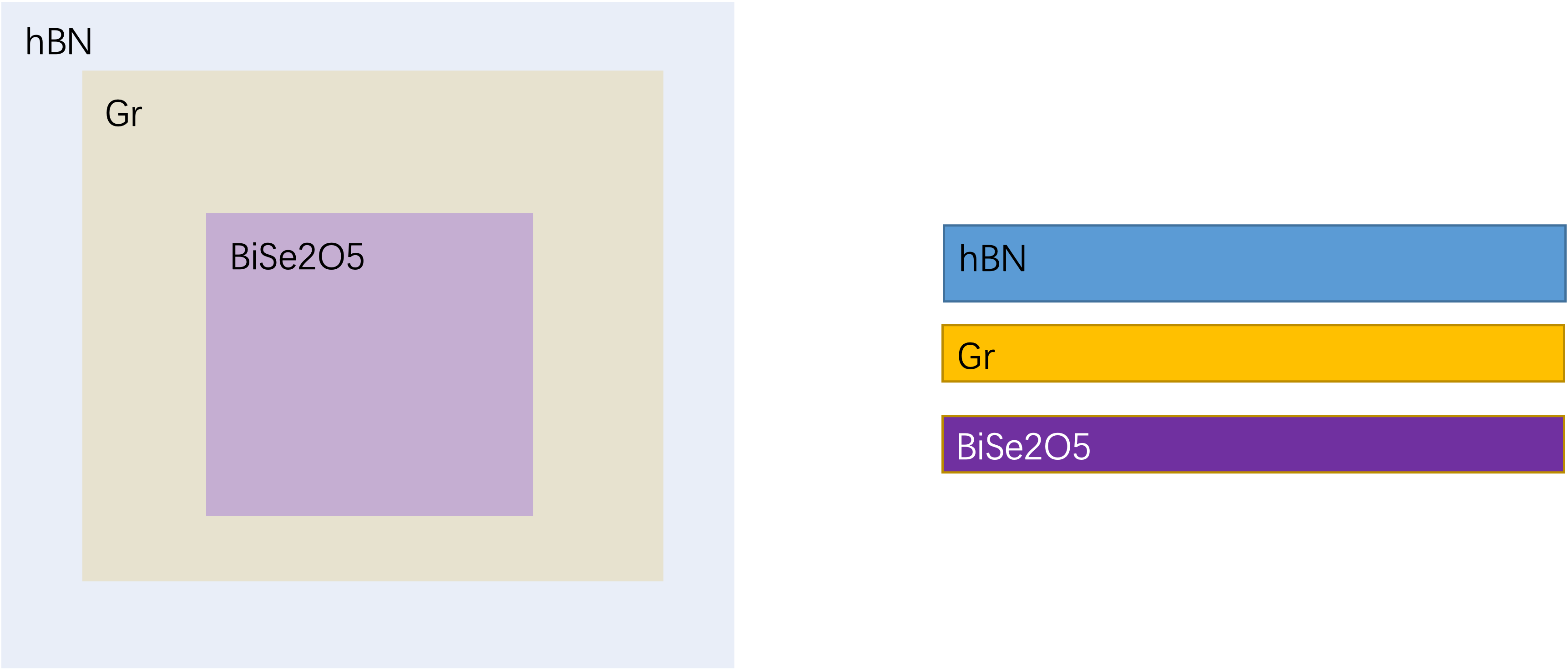 Schematic representation of graphene stacked on BiSe₂O₅
High-quality monolayer graphene, BN and BiSe₂O₅ flakes are mechanically exfoliated onto separate substrates. We employ PC and PDMS transfer methods to stack the graphene onto the BiSe₂O₅ substrate. The device appears as shown:
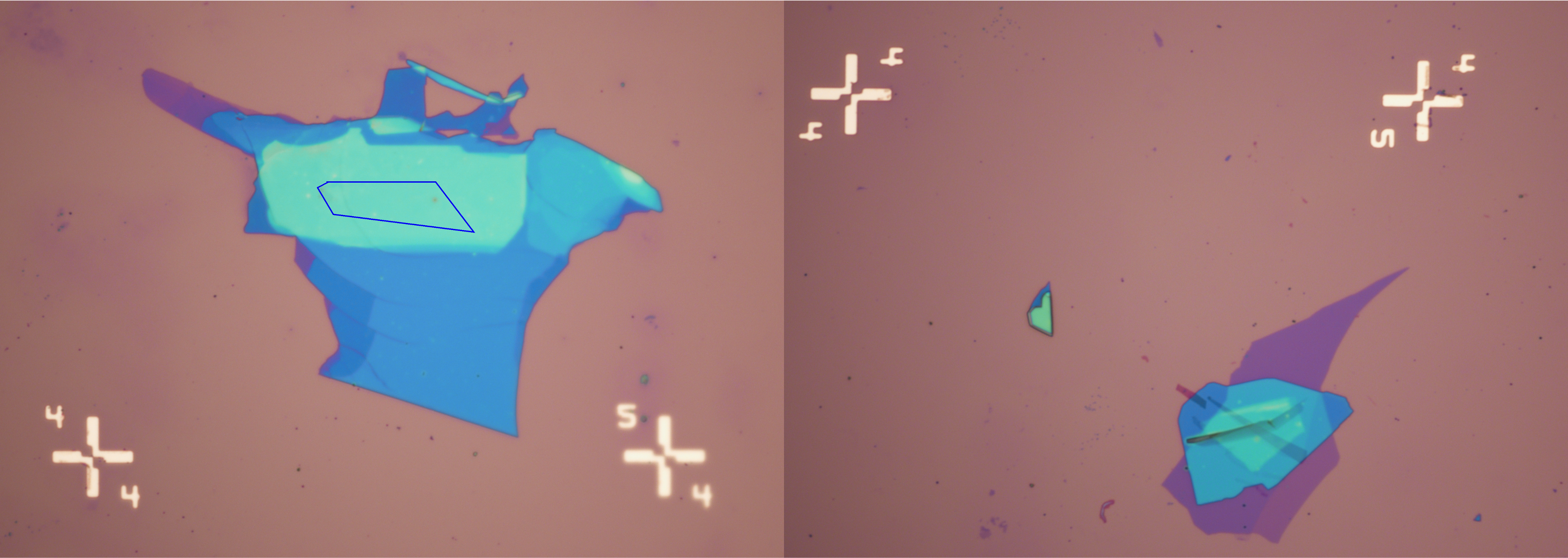 Optical microscope image of the fabricated graphene/BiSe₂O₅ device
To define the electrical contacts and device geometry, we utilized electron beam lithography (EBL) followed by reactive ion etching (RIE) and metal deposition techniques. The finalized device is depicted below:
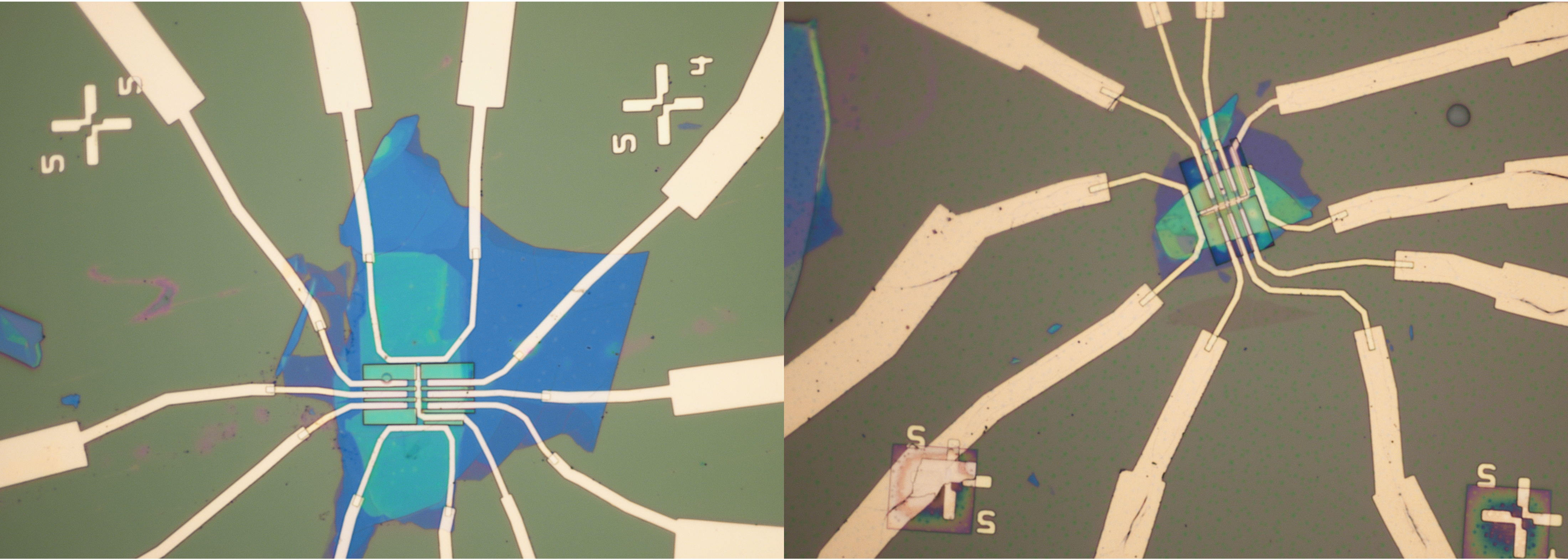 The device after EBL patterning and metal electrode deposition
Measurement Plan
With the device fabricated, the next phase involves comprehensive electrical measurements to characterize the induced SOI. Currently, the device is in queue for measurement due to limited availability of the measurement equipment. In the meantime, theoretical work is being conducted to support the experimental findings.
Conductance Measurements
- Objective: Evaluate the quality of the device by measuring its conductance under different gate voltages.
- Method: Perform field-effect measurements to determine the carrier mobility and ascertain the doping level in the graphene layer.
Magnetoconductance Measurements
- Objective: Investigate the weak anti-localization (WAL) effect to extract spin relaxation times.
- Method: Measure the magnetoconductance under various perpendicular magnetic fields and fit the results using the WAL theoretical model.
Non-local Resistance Measurements
- Objective: Study the spin Hall effect and the inverse spin Hall effect to further understand spin transport properties.
- Method: Measure the non-local resistance as a function of magnetic field and gate voltage, estimating the spin relaxation time using Shubnikov-de Haas (SdH) oscillation frequencies.
Theoretical Calculations
To complement the experimental efforts, theoretical calculations are underway to model the band structure of graphene interfaced with materials exhibiting strong SOI.
- Low-Energy Band Structure Near K/K’ Points: Replicating models of graphene on WS₂ to understand the modifications in the band structure due to the proximity-induced SOI.
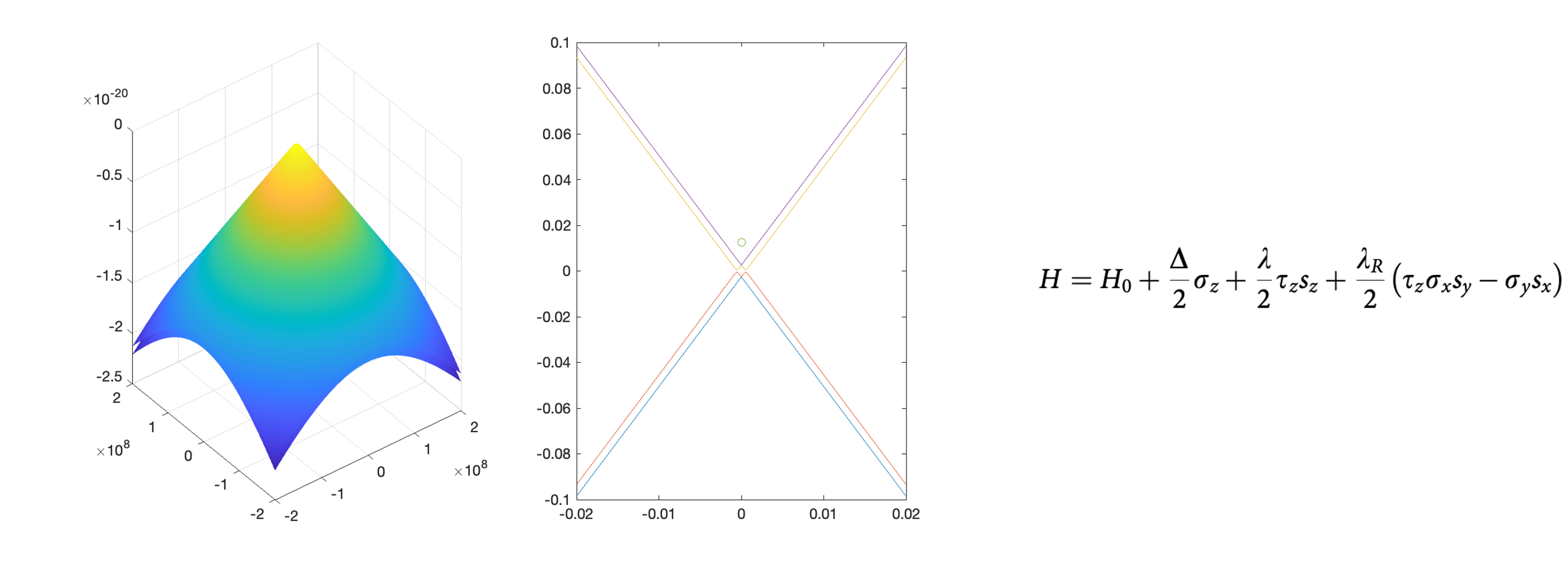 Band Structure and Hamiltonian of graphene on WS₂
- Bilayer Graphene on TMDs: Extending the calculations to bilayer graphene systems to explore potential differences in SOI effects compared to monolayer graphene.
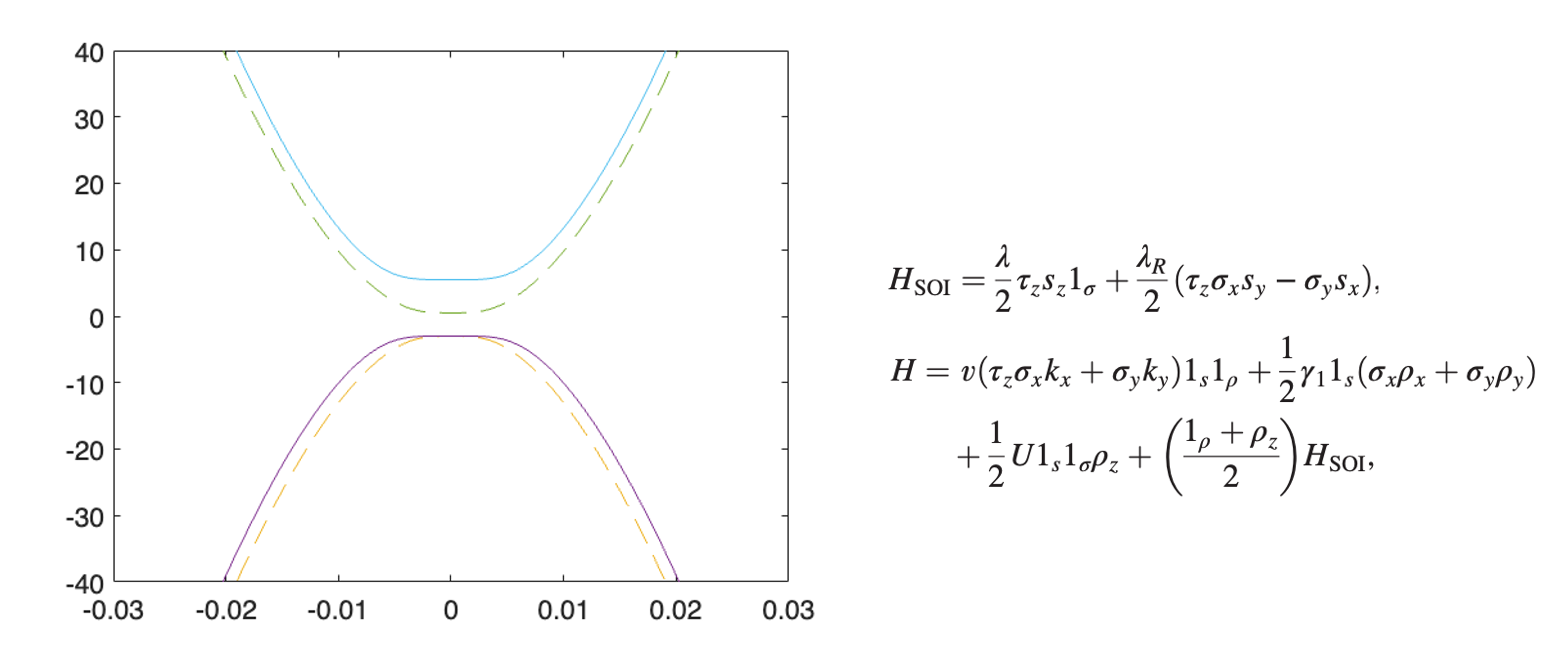 Band Structure and Hamiltonian of bilayer graphene on WSe₂
Computational Methods
- Ab Initio Calculations: Utilizing density functional theory (DFT) to obtain first-principles calculations of the electronic properties.